2018: Joule
https://doi.org/10.1016/j.joule.2017.12.007
Gideon Segev, Hen Dotan, David S. Ellis, Yifat Piekner, Dino Klotz, Jeffrey W. Beeman, Jason K. Cooper, Daniel A. Grave, Ian D. Sharp, Avner Rothschild*
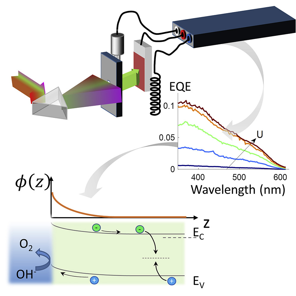
Understanding the optoelectronic and transport properties of semiconductors is essential for producing high-efficiency photovoltaic and photoelectrochemical cells. To this end, empirical extraction of the spatial collection efficiency (i.e., the fraction of photogenerated charge carriers created at a specific point within the device that contribute to the photocurrent) is a useful, nondestructive, analytical tool to study new materials, junctions, and devices. This perspective describes how the spatial collection efficiency can be extracted by combining photocurrent action spectra with optical absorption profiles. The result is high-resolution depth profiles of device functionality with very few assumptions, which paves the way to operando semiconductor tomography. The challenges and opportunities that this method offers for analysis of complex materials are discussed. Since the method is based on widely used spectral response measurements, it can be an important addition to the toolbox of analytical methods for material research for future solar energy conversion systems.
